Thermal Vias: Maximizing Efficiency in PCB Design
The optimal size for these vias is 0.3mm in diameter and should be filled with copper. This size is neither theoretically nor experimentally verified. Since each via offers a slight improvement in temperature, the practical limit for the number of vias ranges from 50 to 100.
Thermal vias must connect the pad to somewhere. This “somewhere” is usually a copper layer located in the stack-up beneath the copper pad. The underlying layer itself reduces the temperature of the copper pad. It is important to recognize which factors more significantly influence the pad's temperature: the thermal via or the underlying copper layer.
Simulation and PCB Examples
The factors described above are investigated using a thermal simulation tool called TRM (Thermal Risk Management). TRM is a simulation software focusing on thermal analysis of PCBs. It can accurately calculate the expected temperature of the PCB based on currents, component heating, and cooling. This tool is ideal for PCB designers and works with single-layer and multi-layer boards, thermal conductors, etc. TRM is easily applicable to ALTIUM Designer, Eagle, OrCAD, Pulsonix, KiCad, and Fusion 360, among others, and does not require knowledge of numerical methods or CAD systems. TRM software by ADAM Research is free for bachelor’s and master’s theses, offering a great opportunity for students and researchers.
For example, consider a PCB made of FR4 material with a thickness of 1600 μm and dimensions of 100 x 100 mm². A thermal component with a copper pad will measure 25 x 25 mm². The advantage of the TRM model is that we can apply a certain number of watts to the copper pad to heat it, avoiding the need to calculate different current flows through all pads, vias, and planes. In this specific case, we apply 2.5 watts to the pad, heating the bare pad to a temperature of 95.7°C – 75.7°C above ambient temperature.
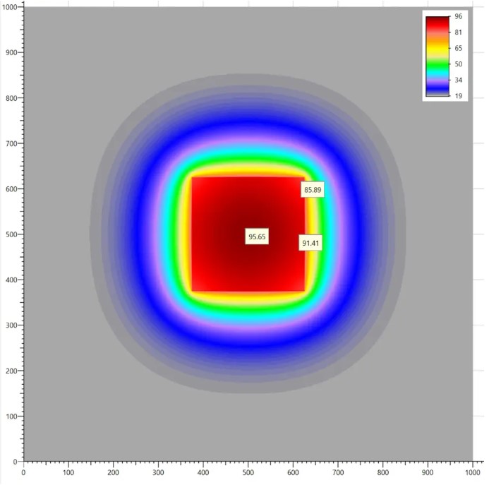
In the study we reference, the temperature of the copper pad is highest in the center and higher at the edges because the corners cool more effectively than the sides of the copper pad, and the sides cool more effectively than the center.
There are nearly unlimited ways to introduce thermal vias into our design, depending on dimensions, materials, the number and size of thermal vias, and heat generation. There is no such thing as a "typical design."
Let's emphasize two key points:
- Thermal via designs almost always terminate on a copper layer of a certain size.
- This copper layer offers greater cooling potential than a series of thermal vias.
The study works with two configurations of copper layers. The "small" layer has the same dimensions as the copper pad. The other layer, called the "large" layer, covers the entire area in one of the board's layers. These copper layers are placed at two depths within the board. One depth is 300 μm "near" the pad, and the other depth is on the "far" side of the board, almost 1.6mm below the pad.
Thermal Vias Performance
Thermal vias will have a diameter of 0.3mm. We will also assume that the thermal vias are filled with plated copper. This allows us to assume that we have the best possible thermal conductivity of the vias.
In the following section, we will compare the thermal conductive properties of the thermal via with the board material. The formula for thermal conductivity, without convection, radiation, and heat spreading, is as follows:
Where:
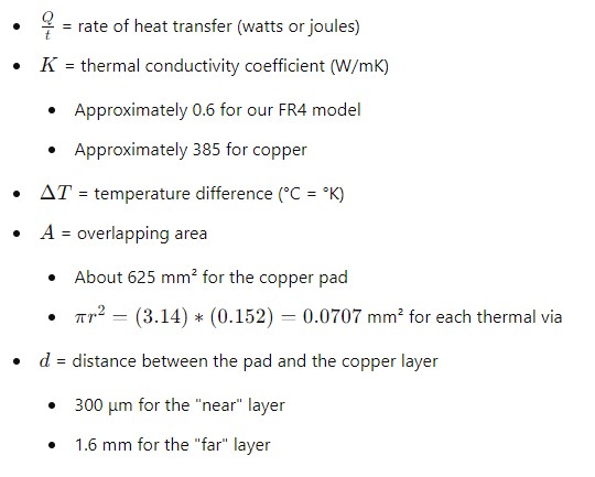
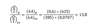
This result indicates that the thermal conductivity through the board material is 13.8 times higher than the thermal conductivity of the thermal via in this specific design. It is crucial to understand a key point. The mere presence of the underlying copper layer reduces the temperature of the copper pad. Therefore, the subsequent thermal conductivity of the thermal via is further diminished.
Simulation Results
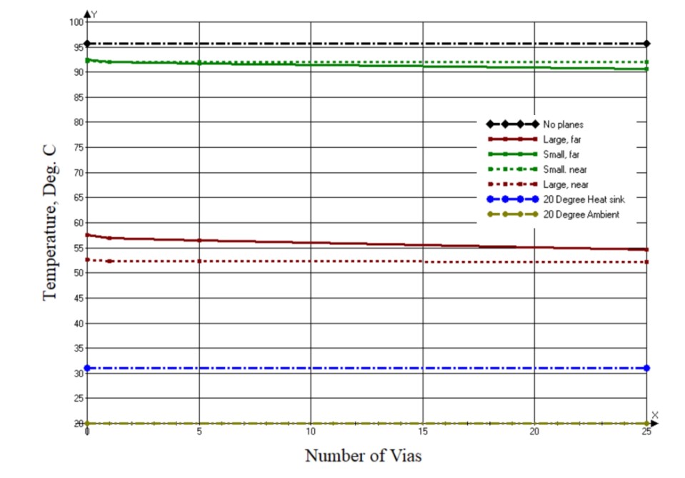
In the referenced study, the simulation results are graphically depicted (see graph). The X-axis shows the number of vias, and the Y-axis shows the pad temperature. This graph indicates that various combinations of layers and thermal vias have a certain impact on the board's maximum temperature.
Layer Dominance
The underlying copper layer significantly reduces the temperature of the copper pad. The combination of the pad and the layer can ensure a stable temperature, depending on the size of the copper layer.
For example, the figure below illustrates the thermal distribution on the lower layer in the case of the "small" copper layer on the far side of the board.
The temperature on this layer is around 80 degrees but quickly drops towards ambient temperature as you move away from the layer. A larger layer with greater cooling capacity tends to lower the pad temperature.
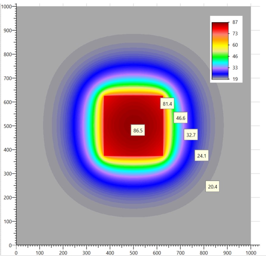
In both cases, the temperature difference between the pad and the layer is relatively small, less than 10°C in our models.
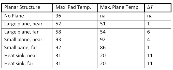
Notes:
- Board arrangement (plane structure)
- Max. temperature of the copper plane
- Max. board temperature
- ΔT remains unchanged (indicating the temperature difference)
- "n/a" indicates data is not available or not applicable.
Thermal Vias = "Point" Solution
The benefit that thermal vias offer is limited to a very narrow area around the via itself. The figure below graphically describes this effect.
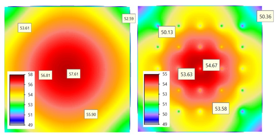
The left side shows the temperature change after adding a large copper layer under the copper pad. The temperature dropped to a maximum of 58°C. After adding 25 thermal vias, with the same board parameters as the left side, the temperature dropped to a maximum of 55°C.
Study Result
Thermal vias result in only a small temperature difference when present or absent, and this difference is localized around the vias themselves. Thermal vias are defined almost entirely by the copper plane to which they are connected. The presence of this copper plane significantly affects the thermal distribution throughout the PCB. This results in a dramatic reduction in the temperature difference (ΔT) between the heated PCB and the copper plane, leading to minimal benefits of thermal vias in reducing temperature.
Furthermore, if the copper surface area is small, the stabilized temperature of the PCB may only be marginally lower than without thermal vias. The greatest effect is observed when using a relatively large copper area, placed on the far side of the board.
In conclusion, any thermal vias added to the board tend to have only a "point" impact, meaning their effect is localized to the site where they are physically placed. This is why many authors emphasize that achieving effective cooling often requires using a large number of thermal vias.
_______________________________________________________________________________
BROOKS, Douglas Brooks a ADAMS, Johannes. PCB Design Guide to Via and Trace Currents and Temperatures. 2021. Norwood: Artech House, 2021. ISBN 9781630818609.
EDN. Online. 2021, vol. 2021, no. 3. AspenCore Logo 9151 E. Panorama Circle, Centennial, CO 80112 United States: https://aspencore.com/, 2021. Dostupné z: https://www.edn.com/pcb-design-a-close-look-at-facts-and-myths-about-thermal-vias/. [cit. 2024-07-08]
Connect with our specialists