Challenges in PCB Design for Space Applications
Who better to advise on such manufacturing than a certified manufacturer and holder of the license for producing PCBs for space, aviation, and military purposes according to the AS9100D standard, such as the Gatema group?
Both the Czech Gatema PCB, focusing primarily on prototype production, and the German Kubatronik Leiterplatten, professionally handling series production, fall under the GATEMA group holding.
Definition and Significance of Space-Qualified PCBs
Space-qualified PCBs, also known as space-grade or radiation-hardened PCBs, are specialized circuit boards designed and manufactured to meet the stringent requirements and extreme conditions of the space environment. These PCBs are built to withstand challenges such as radiation exposure, temperature extremes, mechanical stresses, and the pervasive vacuum. Their significance lies in their crucial role as the backbone of electronic systems in space applications and satellites.
Risk Challenges and Critical Demands for Space Environment PCBs
-
Radiation
Space is permeated with high-energy radiation, including cosmic rays and solar radiation, which can degrade electronic components over time. PCBs must be designed to withstand radiation-induced failures and ensure mission reliability. Standard PCBs are prone to radiation-induced failures, whereas space-qualified PCBs incorporate radiation-resistant materials and designs to withstand exposure and minimize system failures.
-
Temperature Extremes
Spacecraft experience dramatic temperature fluctuations, from the extreme cold of deep space to intense heat during solar exposure. PCBs must be constructed to endure these extremes while maintaining optimal performance. Effective thermal management strategies integrated into PCB design prevent overheating and ensure components operate within specified temperature ranges.
-
Mechanical Stress and Capacity
The launch and re-entry phases subject electronic components to intense mechanical vibrations, shocks, and gravitational forces. PCBs must be robust enough to withstand these stresses without compromising functionality. Spacecraft and satellites have strict size and weight limitations. Space-qualified PCBs are designed with miniaturization in mind, optimizing space utilization while maintaining functionality.
-
Outgassing Control
In the vacuum of space, materials can release volatile compounds in a process known as outgassing. These compounds can contaminate sensitive instruments and optics, highlighting the need for low-outgassing materials in PCB design. Space-grade PCBs use low-outgassing materials to prevent contamination and ensure the integrity of onboard equipment.
-
EMI/RFI Interference
Spacecraft often carry scientific instruments and communication devices sensitive to electromagnetic interference (EMI) and radio-frequency interference (RFI). PCBs should incorporate shielding and filtering techniques to protect these sensitive components.
-
Reliability
Space missions can last years or even decades, requiring flawless reliability of all components, including PCBs. Redundancy and fault-tolerance mechanisms must be integrated into PCB design to ensure uninterrupted operation. Space projects are expensive and irreplaceable. Failure of any onboard electronic system can lead to mission failure. Therefore, PCBs for space projects are designed with an emphasis on reliability, guaranteeing they will function flawlessly in the harsh space environment.
-
Energy Efficiency
Energy is a scarce resource in space. PCBs must be designed to minimize power consumption and maximize the lifespan of onboard batteries or power systems. Space power sources are limited, often relying on solar panels or onboard batteries. PCBs designed for space applications incorporate energy-efficient components and layouts to extend mission duration.
Material Selection for Space-Grade PCBs
Qualified PCBs for space use require careful material selection to withstand harsh space conditions. The production and material selection must focus on two crucial aspects: radiation resistance and thermal properties.
Radiation Resistance
Radiation resistance is a crucial feature in space-grade PCBs. Key materials used in these PCBs for radiation resistance include:
- Radiation-Hardened Semiconductors: These specially designed semiconductors use gate oxides and Insulated Gate Bipolar Transistors (IGBTs) to resist radiation-induced ionization and component degradation.
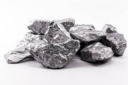
- Ceramic Substrates: Ceramic materials like alumina (Al2O3) or aluminum nitride (AlN) are preferred for PCB substrates. They offer excellent radiation resistance compared to organic substrates.
- Radiation-Hardened Passivation Layers: Passivation layers on semiconductor devices are protected to resist radiation damage, ensuring the continued functionality of active components.
Thermal Properties
Given the extreme temperature variations in space, thermal properties of PCB materials are crucial. The following materials are used:
- Low Thermal Expansion Materials: Materials with low coefficients of thermal expansion (CTE) are preferred. These materials expand and contract less with temperature changes, reducing the risk of solder joint failures and component detachment.
- Thermally Conductive Substrates: Materials like aluminum nitride (AlN) and beryllium oxide (BeO) offer excellent thermal conductivity, allowing efficient dissipation of heat generated by power components.
- High Thermal Stability Insulating Layers: Insulating layers used between conductive layers of PCBs must have high thermal stability to withstand thermal cycles without degrading electrical properties.
PCB Design for Space Applications
PCB design for space applications is also crucial for ensuring the reliability and functionality of electronic systems in harsh space environments. This design requires special attention to several factors.
Reducing EMI and RFI
Electromagnetic interference (EMI) and radio-frequency interference (RFI) can significantly impact the performance of electronic systems in space applications. Techniques to minimize these interferences include:
- Differential Pairs: Transmitting signals over differential pairs can reduce susceptibility to EMI, as interference affects both conductors equally, allowing for easy cancellation.
- Shielding: Using metal shielding layers or enclosures around sensitive components can block unwanted EMI and RFI.
- Filtering: Using filters like LC filters or ferrite beads can help remove unwanted high-frequency noise.

Thermal Management
Effective thermal management is essential to ensure PCB components for space applications do not overheat and remain functional within their operating temperature ranges. Thermal management techniques include:
- Thermally Conductive Materials: Using materials with high thermal conductivity, such as copper for conductive layers and heat sinks, can help dissipate heat away from sensitive components.
- Thermal Vias: Implementing thermal vias that connect different layers of the PCB and help dissipate heat from hot areas.
- Thermal Simulations: Utilizing thermal simulations during PCB design can help identify hot spots and optimize component placement for better heat dissipation.
Material Selection
The choice of materials determines whether the board can withstand the harsh conditions of the space environment. Suitable manufacturing materials include:
- Substrates: Using substrates with high thermal conductivity and low thermal expansion, such as ceramic materials or polytetrafluoroethylene (PTFE).
- Plating: Plating materials must be resistant to corrosion and oxidation processes, such as gold (Au) or palladium (Pd).
- Soldering Materials: Using soldering materials with high-temperature resistance and low susceptibility to outgassing.
Mechanical Strength
Mechanical strength determines whether the PCB can withstand vibrations, shocks, and mechanical stresses during launch and operation. Techniques to enhance mechanical strength include:
- Board Reinforcement: Using reinforcing layers or metal cores to increase PCB rigidity.
- Solder Joints: Using high-quality soldering techniques and materials to ensure strong and durable joints.
- Mechanical Fastening: Using mechanical fasteners such as screws or clamps to secure the PCB and components.
Outgassing
Outgassing in the vacuum of space can negatively impact the performance of electronic systems. Techniques to minimize outgassing include:
- Material Selection: Choosing materials with low outgassing that are tested and approved for space applications.
- Surface Treatments: Using surface treatments that reduce the amount of volatile compounds released.
- Careful Soldering: Utilizing soldering techniques and materials that minimize outgassing during operation.
Adhering to these design techniques and selecting the right materials ensure that PCBs can reliably operate in the demanding conditions of the space environment. These steps not only enhance the durability and lifespan of PCBs but also minimize the risk of mission-critical failures.
Moreover, the use of advanced technologies and innovative testing and validation methods contributes to achieving high standards of quality and reliability. Ultimately, the careful and thorough application of these principles enables the successful implementation of complex space projects and contributes to further development and knowledge in the field of space exploration.
As technology continues to evolve, new challenges and opportunities will inevitably require further improvements and adaptations. However, with a solid foundation in proven PCB design and manufacturing practices, we can confidently face future challenges and continue to expand the boundaries of human knowledge in space.
Here you can see that manufacturing printed circuit boards for space applications is not for everyone who offers PCBs.
Adhering to stringent manufacturing conditions and utilizing special materials alone does not guarantee reliability and safety.
Manufacturers of such boards must undergo a complex certification process involving practically all company departments.
They must optimize production, ensure the security of manufacturing data, and resolve identified discrepancies. Only then can they obtain the AS9100D certification, which ranks them among the manufacturers of electronic components for space applications.
In our case, what is produced in Europe never goes to Asia or other non-European countries, nor does it leave Gatema. Data security is assured as required by the enhanced measures of the AS9100D standard, and we honor this principle throughout the Gatema holding as part of our corporate philosophy.
Connect with our specialists